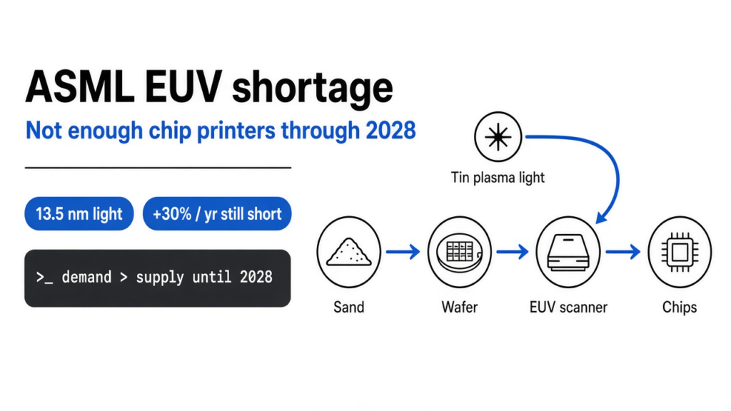
On 14 October 2026, ASML told investors its planned supply of chip-printing machines will not meet customer demand in 2027 or in 2028. The sentence is about a factory schedule, and it is the whole ASML EUV shortage in one line. The reason is a drop of molten tin, fired 50,000 times a second, inside a vacuum.
Hold that sentence. It will mean more after the physics. Then we come back to it, and to what it does not mean.
If you only remember five things
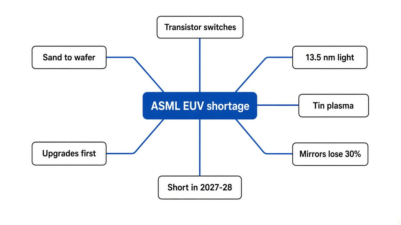
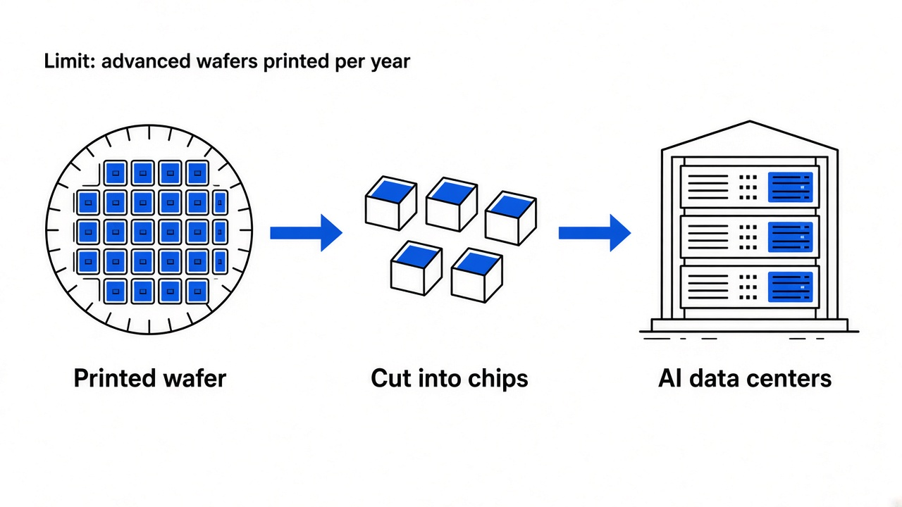
- A chip is a photograph of billions of switches, reprinted many times on a disc of silicon (the purified form of the element in sand).
- The smallest switches need light so short that air and glass swallow it. That light is extreme ultraviolet (EUV, light whose waves are 13.5 nanometers from peak to peak, close to an X-ray).
- ASML is the only company that sells the EUV scanner used in a real high-volume factory. The light is made by exploding a tin droplet with a laser.
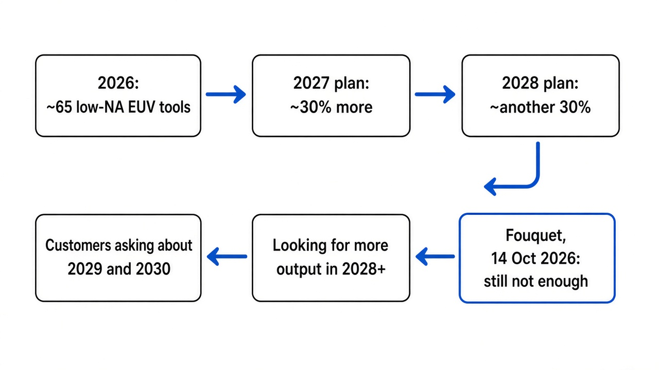
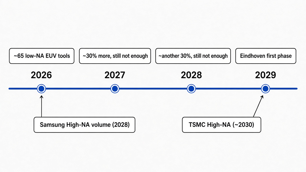
- ASML already planned to build about 30 percent more of these tools in 2027 and another 30 percent in 2028. On this call, chief executive Christophe Fouquet said that is still not enough.
- A new ASML factory building in Eindhoven does not finish its first phase until 2029. The fast relief is upgrades to machines already installed, not a new building.
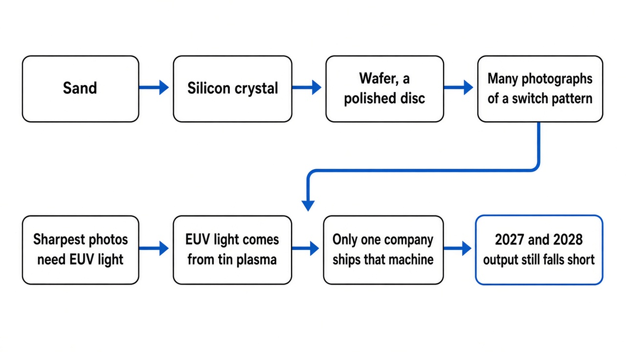
The whole shortage is that chain. Each box below is one step, with the word defined before it is used again.
Start with sand, because the chip is not metal
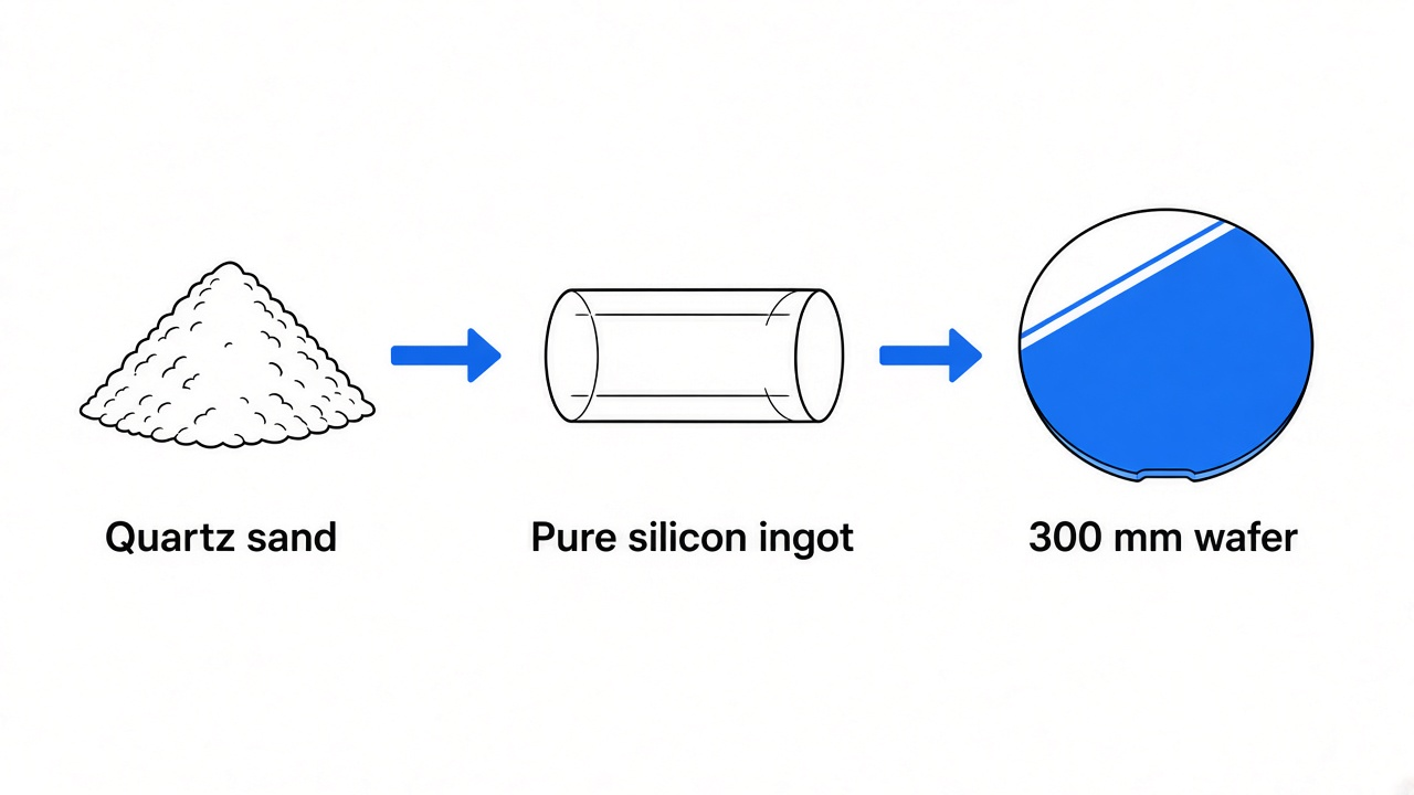
The stuff in a chip starts as sand. Ordinary sand is mostly quartz (a crystal of silicon dioxide, which is silicon atoms locked to oxygen). Chip makers strip the oxygen away until they have silicon that is almost perfectly pure. Pure here means a few foreign atoms in a billion. One stray atom in the wrong place becomes a defect (a spot that does not switch when it should).
That pure silicon is grown into one giant crystal, called an ingot (a sausage-shaped single crystal, so the atoms line up the same way all the way through). A single crystal matters because a jumble of little crystals would scatter electrons (the tiny charged particles that carry current) and the switch would be unreliable.
The ingot is sliced into discs and polished until they look like mirrors. Each disc is a wafer (the blank that many chips are printed on at once, then cut apart). A modern wafer is typically 300 millimeters across, about the size of a dinner plate. The mirror finish is not for looks. The surface has to be flatter than the features that will be printed on it.
A chip is a crowd of switches, not a brain
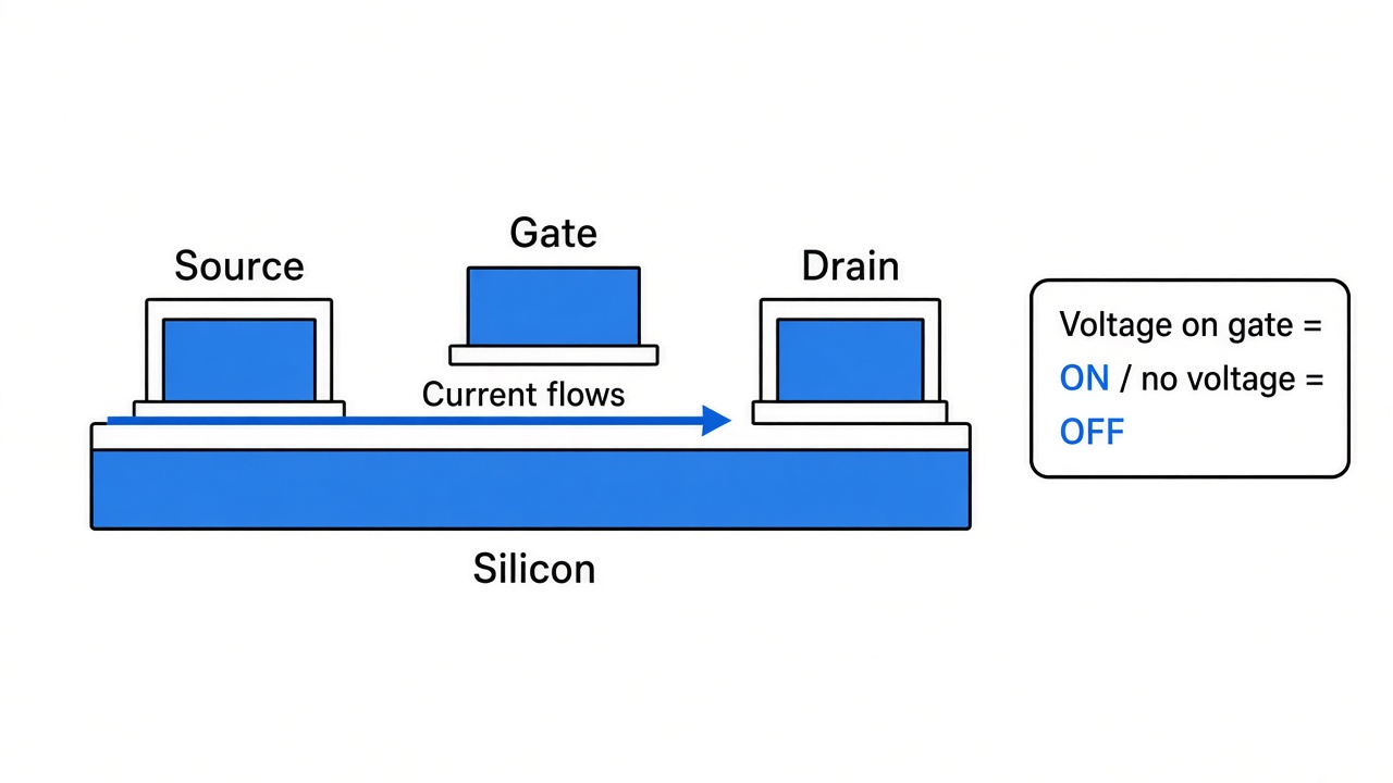
Before the word transistor, picture a switch you can flip with a voltage (an electrical push). On, current flows. Off, it does not. A transistor (that voltage-controlled switch, built into the silicon) is the only moving idea in the chip. There is no tiny gear. Logic, memory, and the math inside an AI model are just huge numbers of these switches opening and closing.
A leading-edge chip holds tens of billions of those switches. You cannot place them with a tweezer. You photograph the pattern onto the wafer, then etch it (eat the unprotected silicon away with chemicals). Then you do it again, for the next layer. A finished chip is a stack of these photographs. The sharpest layers are the ones that need the most expensive light. The rest can use older tools.
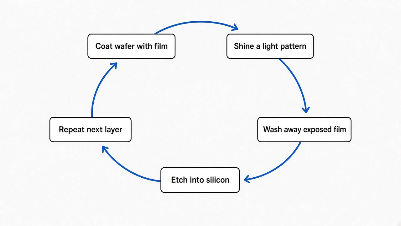
The printing step has a name. Lithography (printing a pattern with light, the way a darkroom print uses a negative, except the paper is the wafer) is that step. The stencil is a reticle (a master plate that holds the circuit drawing). The wafer is coated with photoresist (a film that changes where the light hits, like camera film). After a wash and an etch, the photograph has become a physical shape.
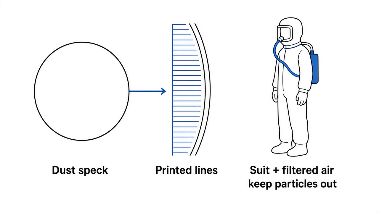
The building those steps happen in is a fab (short for fabrication plant, a chip factory with the air filtered harder than a hospital operating room). People wear a coverall, a hood, and a mask so skin and hair stay out of the air. The shortage in today’s news is not a shortage of coveralls. It is a shortage of the camera.
Light has a size, and that size is the limit
Light is a wave. Wavelength (the distance from one peak of the wave to the next) is how “fat” the light is. You cannot draw a line much thinner than the light you draw it with. A thick marker cannot sign a grain of rice. Ordinary visible light has a wavelength of roughly 400 to 700 nanometers. A nanometer (a billionth of a meter) is the unit. A human hair is about 70,000 nanometers across. The switches on a leading-edge chip are a few tens of nanometers, and the tightest gaps are smaller still.
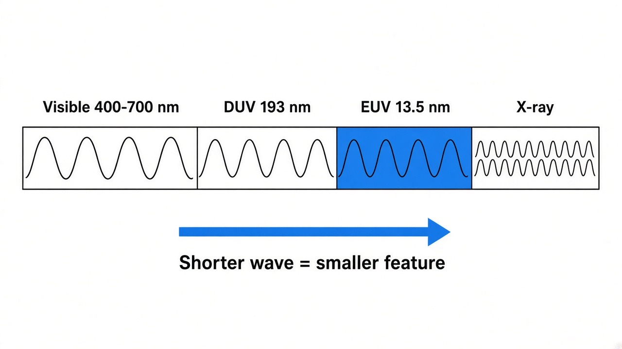
Chip factories spent decades walking down that spectrum. They used ultraviolet, then deep ultraviolet (DUV, ultraviolet at 193 nanometers, which still passes through special glass lenses). They even put a drop of water between the lens and the wafer, called immersion (the water bends the light harder, so the spot gets smaller). That bought a few more generations. It does not buy the smallest layers anymore.
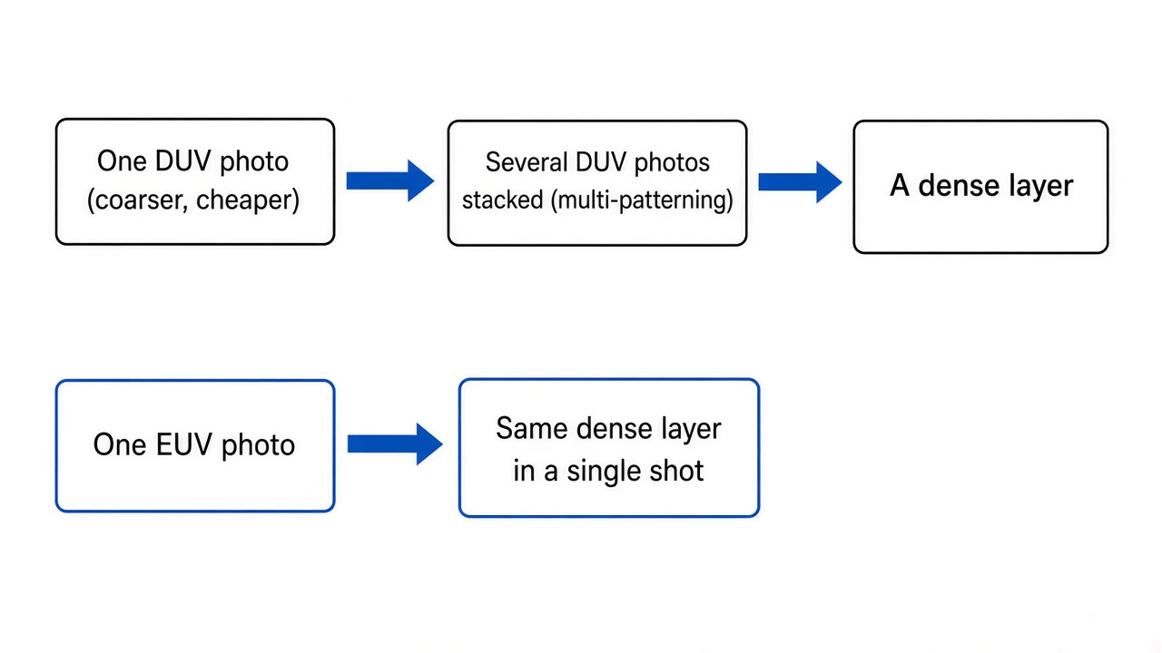
One caution before the formula. A single DUV exposure is not the smallest thing a DUV factory can print. Multi-patterning (splitting one dense pattern into two or more sparser photographs, then lining them up) pushes below that single-shot size. It works. It also costs extra passes, extra time, and extra chances to miss the alignment. EUV exists so the tightest layer can be one photograph instead of several.
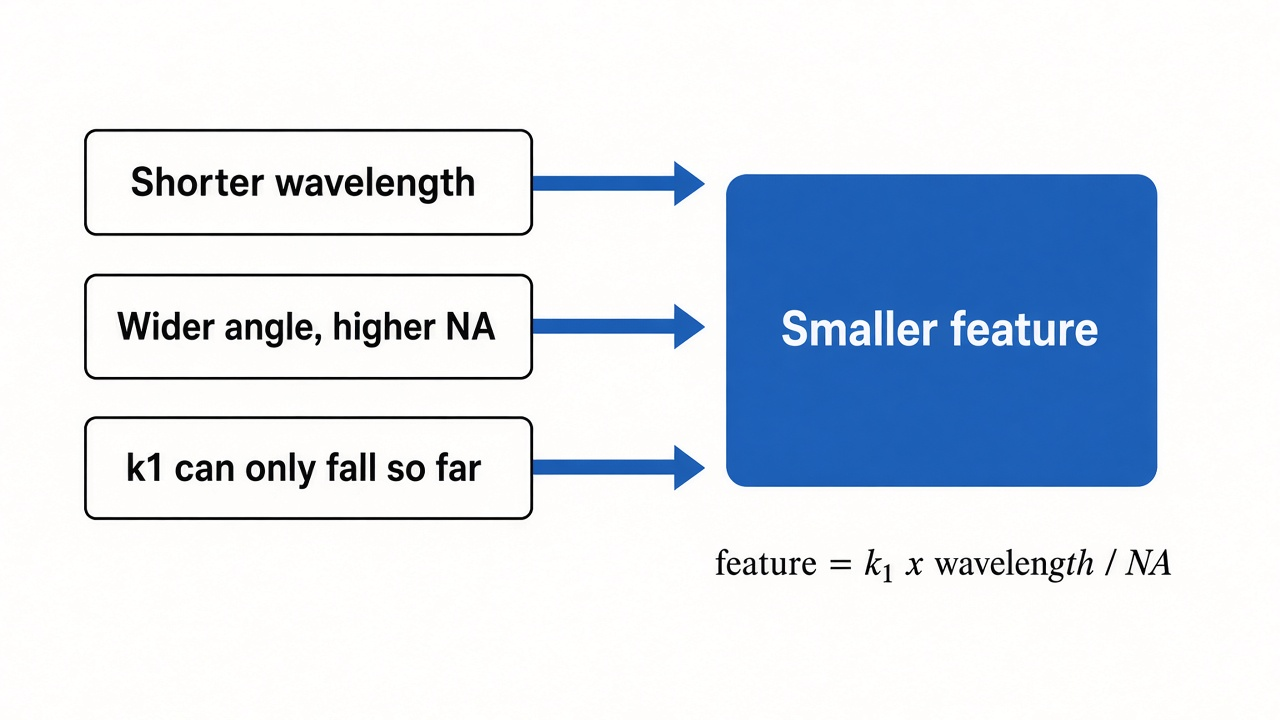
The industry’s printing rule, used for a century of microscopes and cameras, is small and worth doing once by hand:
smallest feature = k1 times wavelength, divided by NA
Each piece, before the letters:
- The smallest feature is the width you are trying to print.
- Wavelength is the fatness of the light, from the last section.
- NA, numerical aperture (how wide an angle of light the lens or mirror collects, written as a number from 0 to 1) is the acceptance angle. A wider cone of light can carry a finer detail, which is why a big camera lens resolves more than a pinhole.
- k1 (a factor for how clever the stencil, the film, and the tricks are) is the part engineers fight over. In a single exposure it struggles to get much below about 0.25. “Try harder” hits a wall.
| Setup | Wavelength | NA | k1 of 0.33, worked by hand |
|---|---|---|---|
| Old DUV immersion | 193 nm | about 1.35, because of the water | 193 times 0.33 divided by 1.35, about 47 nm |
| EUV, low-NA, today’s workhorse | 13.5 nm | 0.33 | 13.5 times 0.33 divided by 0.33, which is 13.5 nm |
| EUV, high-NA, the next machine | 13.5 nm | 0.55 | 13.5 times 0.33 divided by 0.55, about 8 nm |
Read the middle row slowly. The 0.33 on the top and the 0.33 on the bottom cancel. With this k1, low-NA EUV prints a feature of 13.5 nanometers, about as wide as the wavelength itself. High-NA (the same light, collected at a wider angle, NA 0.55) lands near 8 nanometers. That is the whole reason a wider machine exists. The arithmetic is not a slogan. It is the rule above, with the wavelengths and angles these tools actually use. The k1 of 0.33 is a worked example of a capable process, not a law of nature. Push k1 lower and the feature shrinks a bit more, until the single-exposure wall near 0.25.
Why this particular light refuses to go through glass
Thirteen and a half nanometers is not a random pick. Go much longer, and the feature will not shrink, as the table shows. Go much shorter, toward a real X-ray, and you cannot steer the beam. Almost everything absorbs it, including the lenses you would like to use.
EUV is absorbed by air. The path from the lamp to the wafer is a vacuum (a sealed chamber with the air pumped out, so the light is not eaten on the way). EUV is also absorbed by glass. A lens, which is a shaped piece of glass, is useless here. The machine uses mirrors. The useful mirrors at this wavelength are a stack of molybdenum and silicon, and even a good one reflects only about 70 percent of the light. The other 30 percent is lost as heat. A US National Institute of Standards and Technology paper on these mirrors put the peak near 70 percent, and that limit has not been wished away.
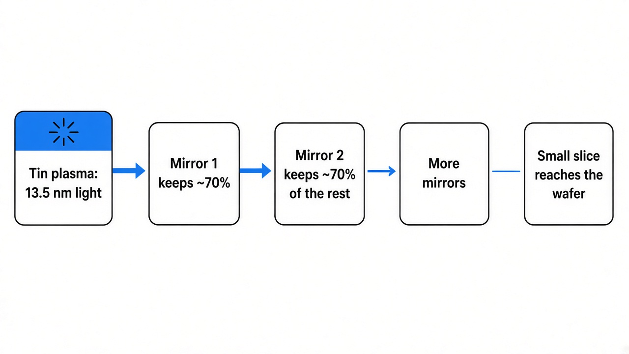
Count it. Two mirrors leave about half the light (0.7 times 0.7 is 0.49). Six mirrors leave about one eighth. The projection optics need several mirrors, and the collector that grabs the light is another. Most of the light never reaches the wafer. That is why the source has to be violent. A dim source means a slow camera. A slow camera means each wafer costs more, and the fab prints fewer of them.
The lamp is an explosion of tin, 50,000 times a second
There is no EUV bulb on a shelf. ASML’s own description of the source, which matches the account its engineers published in IEEE Spectrum, goes like this.
A droplet of molten tin, about 30 microns across, falls through the chamber. A micron (a millionth of a meter) makes that droplet about half the width of a hair. A first, gentler laser pulse hits it and flattens it into a pancake. A flat target gives more useful light than a ball. A second, harder pulse from a carbon-dioxide laser (a laser whose light is made in carbon dioxide gas) vaporizes the pancake into a plasma (a gas so hot that electrons are torn off the atoms, so it glows). ASML describes that plasma as about 40 times hotter than the surface of the Sun. The glow peaks at 13.5 nanometers, which is exactly the color the mirrors know how to reflect. Then a rush of hydrogen sweeps the tin debris away, so it does not coat the mirrors and blind them.
This happens about 50,000 times a second. Not because it is dramatic. Because anything slower does not make enough light to keep the wafers moving.
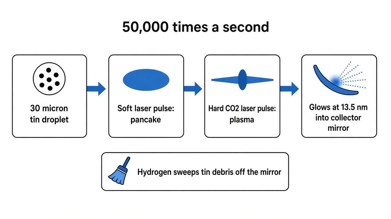
Now loop back. Lithography needed short light. Short light cannot use a lens. The mirror that replaces the lens only works at 13.5 nanometers. Tin plasma happens to glow there. So the most advanced chips on earth depend on a microscopic tin drip, hit accurately, 50,000 times a second, inside a vacuum, for months, without the mirror going dull. That is the machine ASML says it cannot build fast enough.
Two machines, not one
Low-NA is the workhorse. NA 0.33, a feature of 13.5 nanometers in the worked example above, already in factories. Fouquet said ASML expects to ship about 65 of these low-NA EUV systems in 2026, more than 50 percent more than in 2025. In July the company had already described 2026 low-NA capacity as around 65.
High-NA is the wider-angle machine, NA 0.55, near 8 nanometers in the same arithmetic. It is not a lab toy anymore, and it is not the volume tool of 2026 either. On this call Fouquet separated the customers:
- Intel is already running High-NA in high-volume manufacturing (a real production line, not a demo) and is increasing the number of layers it uses the tool for.
- Samsung, he said, will use High-NA in high-volume manufacturing starting in 2028.
- TSMC has asked ASML to lead a group bringing a larger, 12-inch reticle to the industry in the first half of the next decade, and Fouquet said TSMC has confirmed it will introduce High-NA in high-volume manufacturing around 2030.
A bigger reticle matters because High-NA’s wider angle sees a smaller patch of the wafer at a time. A larger stencil lets you print a big chip without stitching two exposures together as often. Stitching (lining up two photographs so they meet without a seam) is a place defects are born.
The volume problem in the 2027 and 2028 warning is mostly the low-NA workhorse, plus the deep-ultraviolet immersion tools that still print the layers EUV is not used for. High-NA is a second hill, climbed by a few customers on different years.
Now the earnings sentence means something
ASML’s third-quarter slides, published 14 October 2026, are the easy half of the day.
| Item | Figure | What it is |
|---|---|---|
| Q3 total net sales | €11.7 billion | Machines plus service |
| Q3 net income | €5.0 billion | Profit after costs and tax |
| Q3 gross margin | 57.5 percent | Share of sales left after the direct cost of building and supporting the tools |
| Earnings per share | €12.95 basic | Profit divided by shares |
| Lithography systems sold | 121 | All light types, not just EUV |
| Installed-base sales | about €3.3 billion | Service and upgrades on machines already in fabs |
| Q4 sales guide | €14.2 to €15.2 billion | Next quarter |
| Full-year 2026 sales | €44 to €45 billion | In July the floor was €43 billion |
| Full-year gross margin | around 56 percent | In July the range was 54 to 56 percent |
Do not read 121 as 121 EUV machines. About 65 low-NA EUV systems for the whole year is roughly 16 a quarter. The quarter’s 121 lithography systems are mostly older-light tools: immersion, and the still-older lamps used for coarser layers. The scarce camera is the small slice.
Chief financial officer Roger Dassen put 2026 in one comparison. Sales are expected to be about 36 percent higher than 2025. The EUV business grows over 45 percent. China is expected to be about 20 percent of the year’s business, so this is not a single-country order book.
Christophe Fouquet, on the 14 October 2026 call: “Today they expect that their supply will not meet the demand at least until 2028.” He was talking about his customers, the chip factories. Then, about ASML’s own tools: “30 percent in 2027, 30 percent in 2028 will not allow us to meet our customer demand. So we have to do more.”
Those are two shortages stacked. The fabs cannot print as many advanced chips as their customers want, at least through 2028. And ASML cannot hand the fabs as many cameras as the fabs now want, even after growing shipments about 30 percent in 2027 and again in 2028. The July plan was to add 30 percent to the 2026 low-NA EUV base of about 65, and the same shape of increase for deep-ultraviolet immersion tools, of which 2026 capacity was about 130. Today he said that plan falls short, and that ASML is looking for more capacity especially in 2028 and after.
He also said a lot of order talk has moved past 2027. There is heavy order intake for 2028, and “some strong interest to already place orders for 2029 and sometimes even 2030.” Interest is not a booked order. It is evidence that customers are treating these machines like inventory they are afraid to be without.
Why a new building does not fix 2027
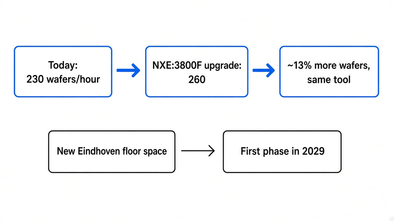
You cannot hire a weekend shift and double this. The mirrors are a craft industry of their own. The laser has to hit a 30-micron droplet in the center, then hit the pancake, tens of thousands of times a second, for the life of the tool. The finished scanner is shipped in many crates and then qualified inside the customer’s fab, which itself takes months. ASML, on 8 September 2026, started construction of a new Eindhoven campus, BIC North, to expand manufacturing. The company said the first phase is expected to be completed in 2029.
Read that against the warning. The building that is supposed to add room does not finish its first phase until the year after the shortage Fouquet just described. Capacity in 2027 and 2028 has to come from the buildings, the suppliers, and the tools already in motion.
The fast patch is a faster machine you already own
Installed-base sales, the service and upgrade line, were about €3.3 billion of this quarter’s €11.7 billion. That is the unglamorous lever, and it is the one that moves before 2029.
Dassen described the next productivity step on the current low-NA tool, the NXE:3800F (ASML’s model name for that scanner). It goes from 230 wafers per hour today to 260 wafers per hour. It shows up in small numbers in 2027, and it matters for customer capacity in 2028 and after. On the immersion side, the critical deep-ultraviolet tools shipped in 2027 are planned at 330 wafers per hour.
Thirty extra wafers an hour sounds small next to “30 percent more machines.” It is not small. A fab that already owns the scanner does not wait for Eindhoven. It waits for a field upgrade. Across a fleet, 230 to 260 is about 13 percent more wafers from the same footprint, if the rest of the line can keep up. Often the rest of the line cannot, which is why this is relief, not a cure.
What this does not mean
It does not mean phones stop, or that models already trained go dark. Chips that exist, keep existing. It does not mean every semiconductor is scarce. Cars, power supplies, and a lot of sensors are printed with older light, on tools sold by ASML and also by Nikon and Canon. The monopoly, if you use that word, is specifically on EUV scanners for high-volume manufacturing. It is not a monopoly on “chips.”
It does not mean a clever chip design escapes the camera. An accelerator (a chip built to do the matrix math in an AI model, instead of doing every job a general processor does) still has to be printed. A custom design can use each wafer better. It cannot invent a second ASML.
It also does not mean the price of using AI only goes up. Memory is a separate squeeze, covered in why PCs cost more in 2026. Fabs will run the machines they have harder, shift the most expensive layers onto EUV and leave the rest on immersion, and sell every good wafer they can print. The constraint is the slope: how fast the number of leading-edge wafers can grow between now and 2028. Fouquet’s customers have already told him their own supply misses demand at least until then.
What is worth watching next
- Whether ASML puts a number on “more than 30 percent” for 2028, or stays at “we are looking.”
- Whether the 2029 and 2030 interest turns into orders with dates and deposits.
- The fourth-quarter landing. The guide is €14.2 to €15.2 billion of sales and a gross margin around 57 percent. Installed-base sales around €3.7 billion would mean upgrades are still doing real work.
- High-NA as three different clocks: Intel adding layers now, Samsung in 2028, TSMC around 2030. If those years slip, the low-NA workhorse has to carry even more of the shrink.
- The Eindhoven date. A 2029 first phase cannot print a 2027 wafer.
An interim dividend of €1.88 a share is payable on 4 November 2026. That is a capital-return detail, not a capacity detail. The capacity detail is the tin droplet.
Common questions about the ASML EUV shortage
What is the ASML EUV shortage?
On 14 October 2026, ASML said its planned output of EUV scanners will not meet customer demand in 2027 or 2028, even after growing about 30 percent in 2027 and another 30 percent in 2028 from a 2026 base of about 65 low-NA systems. Its customers, the chip factories, also expect their own supply to miss demand at least until 2028.
Why can ASML not just build more EUV machines?
Each scanner depends on precision molybdenum-silicon mirrors, a laser that hits a 30-micron tin droplet about 50,000 times a second, and months of qualification inside the customer’s fab. The new Eindhoven campus, BIC North, does not finish its first phase until 2029.
Does the EUV shortage mean every chip will be scarce?
No. Cars, power supplies, and many sensors are printed with older light on tools from ASML, Nikon, and Canon. The squeeze is on leading-edge wafers, and the fastest relief is upgrades to installed tools, such as the NXE:3800F going from 230 to 260 wafers an hour.